Find the galvanic isolation diagram for the network. Fast switching and galvanic isolation: optoelectronic relays FROM IR. Power decoupling methods
The series of articles consists of three parts:
Interference in circuits.
During normal operation of an electronic device, interference may occur in the circuit.
Interference can not only interfere with the normal operation of the device, but also lead to its complete failure.
Rice. 1. Interference in the useful signal.
You can see the interference on the oscilloscope screen by connecting it to the part of the circuit under study (Fig. 1). The duration of interference can be either very short (a few nanoseconds, so-called “needles”) or very long (several seconds). The shape and polarity of the interference also varies.
The propagation (passage) of interference occurs not only along the wired connections of the circuit, but sometimes even between parts of the circuit that are not connected by wiring. In addition, interference can overlap and add up to each other. Thus, a single weak interference may not cause a malfunction in the device circuit, but the simultaneous accumulation of several weak random interferences leads to incorrect operation of the device. This fact makes the search and elimination of interference many times more difficult, since it takes on an even more random nature.
Sources of interference can be roughly divided:
- External source of interference. A strong electromagnetic or electrostatic field source near the device may cause the electronic device to malfunction. For example, a lightning discharge, relay switching of high currents or electric welding.
- Internal source of interference. For example, when you turn on/off a reactive load (an electric motor or an electromagnet) in a device, the rest of the circuit may malfunction. An incorrect program algorithm can also be a source of internal interference.
To protect against external interference, the structure or its individual parts are placed in a metal or electromagnetic shield, and circuit solutions with less sensitivity to external interference are also used. The use of filters, optimization of the operating algorithm, changes in the construction of the entire circuit and the location of its parts relative to each other help against internal interference.
What is considered very elegant is not the indiscriminate suppression of all interference, but the deliberate direction of them to those places in the circuit where they will fade out without causing harm. In some cases, this path is much simpler, more compact and cheaper.
Assessing the probability of interference in circuits and ways to prevent them is not a simple task, requiring theoretical knowledge and practical experience. But nevertheless, we can firmly say that the probability of interference increases:
- with an increase in switched current or voltage in the circuit,
- with increasing sensitivity of parts of the circuit,
- with an increase in the performance of the used parts.
In order not to redo the finished design due to frequent failures, it is better to become familiar with the possible sources and paths of interference at the circuit design stage. Since about half of all manifestations of interference are associated with “bad” power supply, it is best to start designing a device by choosing a method for powering its parts.
Interference in power supply circuits.
Figure 2 shows a typical block diagram of an electronic device, which consists of a power source, control circuit, driver and actuator.
Most of the simplest robots from the series on this site are built according to this scheme.

Rice. 2. Joint power supply of the control and power parts.
In such circuits we can conditionally distinguish two parts: control and power. The control part consumes relatively little current and contains any control or computing circuits. The power section consumes significantly more current and includes an amplifier and termination load.
Let's look at each part of the circuit in more detail.
Rice. 2 a.
Power supply(Fig. 2 a.) can be “batteries” or a mains transformer power supply. The power supply may also include a voltage stabilizer and a small filter.
Rice. 2 b.
Control circuit- this is part of the circuit (Fig. 2 b.), where any information is processed in accordance with the operation of the algorithm. Signals from external sources, for example, from some sensors, can also come here. The control circuit itself can be assembled using microcontrollers or other microcircuits, or using discrete elements.
Communication lines they simply connect the control circuit to the driver-executive device, that is, these are just wiring or tracks on a printed circuit board.
Rice. 2nd century
Actuator(Fig. 2 c.) is often a mechanism that converts an electrical signal into mechanical work, such as an electric motor or electromagnet. That is, the actuator converts electrical current into another form of energy and usually consumes a relatively large current.
Rice. 2 years
Since the signal from the control circuit is very weak, so driver or amplifier(Fig. 2 d) is an integral part of many schemes. The driver can be made, for example, using only a transistor or a special chip, depending on the type of actuator.
As a rule, the main source of strong interference is the actuator. The interference that appears here, having passed through the driver, spreads further along the power bus (The interference in Fig. 2 is shown schematically by an orange arrow). And since the control circuit is powered from the same power source, there is a high probability that this interference will affect it as well. That is, for example, an interference that appears in the motor will pass through the driver and can lead to a failure in the control circuit.
In simple circuits, it is enough to place a large capacitor of about 1000 μF and a ceramic 0.1 μF capacitor in parallel with the power source. They will act as a simple filter. In circuits with consumption currents of about 1 ampere or more, to protect against strong interference of complex shapes, you will have to install a bulky, complex filter, but this does not always help.
In many circuits, the easiest way to get rid of the effects of interference is to use separate power supplies for the control and power parts of the circuit, that is, the use of the so-called separate power supply.
Although separate power supply is used not only to combat interference.
Separate meals.
In Fig. Figure 3 shows a block diagram of a certain device. This circuit uses two power supplies. The power part of the circuit is powered from power supply 1, and the control circuit is from power supply 2. Both power sources are connected by one of the poles; this wire is common to the entire circuit and signals are transmitted relative to it along the communication line.

Rice. 3. Separate power supply for the control and power parts.
At first glance, such a circuit with two power supplies looks cumbersome and complex. In fact, such separate power supply circuits are used, for example, in 95% of all household equipment. Separate power supplies there are just different windings of transformers with different voltages and currents. This is another advantage of separate power supply circuits: several units with different supply voltages can be used in one device. For example, use 5 volts for the controller, and 10-15 volts for the motor.
If you look closely at the diagram in Fig. 3, it is clear that interference from the power part does not have the opportunity to get into the control part via the power line. Consequently, the need to suppress or filter it completely disappears.

Rice. 4. Separate power supply with stabilizer.
In mobile structures, for example, mobile robots, due to their size, it is not always convenient to use two battery packs. Therefore, separate power supply can be built using one battery pack. The control circuit will be powered from the main power source through a stabilizer with a low-power filter, Fig. 4. In this circuit, you need to take into account the voltage drop across the stabilizer of the selected type. Typically a battery pack with a higher voltage than the voltage required for the control circuit is used. In this case, the functionality of the circuit is maintained even when the batteries are partially discharged.

Rice. 5. L293 with separate power supply.
Many driver chips are specifically designed for use in circuits with separate power supply. For example, the well-known L293 driver chip ( Rice. 5) has a conclusion Vss- for powering the control circuit (Logic Supply Voltage) and output Vs- to power the final stages of the power driver (Supply Voltage or Output Supply Voltage).
In all robot designs with a microcontroller or a logic chip from the series, L293 can be switched on with a separate power supply circuit. In this case, the power supply voltage (voltage for the motors) can be in the range from 4.5 to 36 volts, and the voltage on Vss can be supplied the same as to power the microcontroller or logic chip (usually 5 volts).
If the power supply to the control part (microcontroller or logic chip) occurs through a stabilizer, and the power supply to the power part is taken directly from the battery pack, then this can significantly save energy losses. Since the stabilizer will only power the control circuit, and not the entire structure. This - Another advantage of separate power supply: energy saving.
If you look again at the diagram in Figure 3, you will notice that in addition to the common wire (GND), the power section is also connected to the control circuit by communication lines. In some cases, these wires can also carry interference from the power part into the control circuit. In addition, these communication lines are often highly susceptible to electromagnetic influences (“noise”). You can get rid of these harmful phenomena once and for all by using the so-called galvanic isolation.
Although galvanic isolation is also used not only to combat interference.
Galvanic isolation.
At first glance, this definition may seem incredible!
How can a signal be transmitted without electrical contact?
In fact, there are even two ways that allow this.
Rice. 6.
Optical signal transmission method based on the phenomenon of photosensitivity of semiconductors. For this, a pair of an LED and a photosensitive device (phototransistor, photodiode) is used, Fig. 6.

Rice. 7.
The LED-photodetector pair is located in isolation in one housing opposite each other. This is what this detail is called. optocoupler(foreign name optocopler), Fig. 7.
If current is passed through the optocoupler LED, the resistance of the built-in photodetector will change. This is how contactless signal transmission occurs, since the LED is completely isolated from the photodetector.
Each signal transmission line requires a separate optocoupler. The frequency of the optically transmitted signal can range from zero to several tens to hundreds of kilohertz.
Rice. 8.
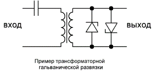
Inductive signal transmission method is based on the phenomenon of electromagnetic induction in a transformer. When the current changes in one of the windings of the transformer, the current in its other winding changes. Thus, the signal is transmitted from the first winding to the second (Fig. 8). This connection between the windings is also called transformer, and a transformer for galvanic isolation is sometimes called isolation transformer.
![]()
Rice. 9.
Structurally, transformers are usually made on a ring ferrite core, and the windings contain several tens of turns of wire (Fig. 9). Despite the apparent complexity of such a transformer, you can make it yourself in a few minutes. Ready-made small-sized transformers for galvanic isolation are also sold.
Each signal transmission line requires a separate such transformer. The frequency of the transmitted signal can range from several tens of hertz to hundreds of thousands of megahertz.
Depending on the type of signal being transmitted and the circuit requirements, you can choose either transformer or optical galvanic isolation. In circuits with galvanic isolation, special converters are often installed on both sides to coordinate (connect, interface) with the rest of the circuit.
Let us now consider the block diagram using galvanic isolation between the control and power parts in Figure 10.

Rice. 10. Separate power supply and galvanic isolation of the communication channel.
From this diagram it can be seen that any interference from the power part has no way of penetrating into the control part, since there is no electrical contact between the parts of the circuit.
The absence of electrical contact between parts of the circuit in the case of galvanic isolation allows you to safely control actuators with high voltage power. For example, a control panel powered by a few volts can be galvanically isolated from a phase network voltage of several hundred volts, which increases safety for operating personnel. This is an important advantage of galvanic isolation circuits.
Control circuits with galvanic isolation can almost always be found in critical devices, as well as in pulsed power supplies. Especially where there is even the slightest chance of interference. But even in amateur devices, galvanic isolation is used. Since a slight complication of the circuit by galvanic isolation brings complete confidence in the uninterrupted operation of the device.
Galvanic isolation or galvanic isolation is the general principle of electrical (galvanic) isolation of the electrical circuit in question in relation to other electrical circuits. Thanks to galvanic isolation, it is possible to transfer energy or a signal from one electrical circuit to another electrical circuit without direct electrical contact between them.
Galvanic isolation makes it possible to ensure, in particular, the independence of the signal circuit, since an independent current circuit of the signal circuit is formed relative to the current circuits of other circuits, for example, the power circuit, during measurements and in feedback circuits. This solution is useful for ensuring electromagnetic compatibility: noise immunity and measurement accuracy are increased. Galvanic isolation of the input and output of devices often improves their compatibility with other devices in harsh electromagnetic environments.
Of course, galvanic isolation also ensures safety when people work with electrical equipment. This is one measure, and the isolation of a particular circuit must always be considered in conjunction with other electrical safety measures, such as protective earthing and voltage and current limiting circuits.
To ensure galvanic isolation, various technical solutions can be used:
inductive (transformer) galvanic isolation, which is used in and for isolating digital circuits;
optical isolation by means of an optocoupler (optocoupler) or optorelay, the use of which is typical for many modern switching power supplies;
capacitive galvanic isolation, when the signal is supplied through a capacitor of a very small capacitance;
electromechanical isolation by means of, for example, .

Currently, two options for galvanic isolation in circuits are very widespread: transformer and optoelectronic.

The construction of transformer-type galvanic isolation involves the use of a magnetic induction element (transformer) with or without a core, the output voltage removed from the secondary winding of which is proportional to the input voltage of the device. However, when implementing this method, it is important to take into account the following disadvantages:
the output signal may be affected by interference generated by the carrier signal;
frequency modulation of the decoupler limits the transmission frequency;
large dimensions.

The development of semiconductor device technology in recent years has expanded the possibilities for constructing optoelectronic decoupling units based on optocouplers.
The principle of operation of the optocoupler is simple: the LED emits light, which is perceived by the phototransistor. This is how galvanic isolation of circuits is carried out, one of which is connected to the LED, and the other to the phototransistor.
This solution has a number of advantages: a wide range of decoupling voltages, up to 500 volts, which is important for building data input systems, the ability to operate decouplers with signals with frequencies up to tens of megahertz, and small dimensions of components.
If galvanic isolation is not used, the maximum current flow between circuits is limited only by relatively small electrical resistances, which can result in the flow of equalizing currents that can cause harm to both circuit components and people touching unprotected equipment. An isolation device specifically limits the transfer of energy from one circuit to another.
Introduction
Galvanic isolation (isolation), commonly referred to simply as decoupling, is a method by which individual parts of an electrical system can be at different ground potentials. The two most common reasons for creating decoupling are for safety from faults in industrial-grade products, and where wired communication is required between devices, each of which has its own power supply.
Power decoupling methods
Transformers
The most common form of decoupling is the use of a transformer. When designing a power stabilization circuit where decoupling is required, the isolating part of the design is associated with the need to increase/decrease the voltage level and is not considered as a separate part of the system. In the event that it is necessary to isolate the entire electrical system (for example, many automotive test equipment requires power supplies to be isolated from the AC mains), a 1:1 transformer can be installed in series with the system to provide the necessary isolation.
Figure 1 - Assortment of SMD transformers
Capacitors
A less common method of creating decoupling is to use capacitors in series. Because of the ability of AC signals to flow through capacitors, this method can be an effective way to isolate parts of an electrical system from the AC mains. This method is less reliable than the transformer method because if a fault occurs, the transformer breaks the circuit and shorts the capacitor. One of the purposes of creating galvanic isolation from the AC mains is to ensure that in the event of a fault, the user is safe from a functioning unlimited current source.
Figure 2 - Example of using capacitors to create decoupling
Signal Isolation Methods
Opto-isolators
When a signal is required to pass between two parts of a circuit at different ground potentials, a popular solution is an opto-isolator (optocoupler). The opto-isolator is a phototransistor that opens (“turns on”) when the internal LED is energized. The light emitted by the internal LED is the signal path and thus the isolation between ground potentials is not broken.
Figure 3 - Diagram of a typical opto-isolatorHall sensor
Another method of transmitting information between electrical systems with separate ground potentials is the use of a sensor based on the Hall effect. The Hall sensor detects induction non-invasively and does not require direct contact with the signal of interest and does not violate the insulating barrier. The most common use of passing inductive information through circuits at different ground potentials is in current sensors.
Figure 4 - Current sensor used to measure current through a conductor
Conclusion
Galvanic isolation (isolation) is the separation of electrical systems/subsystems that may not carry direct current and may have different ground potentials. Isolation can be divided into main categories: power and signal. There are several ways to achieve decoupling, and depending on the project requirements, some methods may be preferable to others.
Case Study
 Figure 5 - PoE (Power over Ethernet) project diagram based on the TPS23753PW controller
 In the diagram above, several transformers and an opto-isolator are used to create a switching power supply, which is used in Ethernet PD (Powered Device) devices. Connector J2 has internal magnets that isolate the entire system from the PoE source. T1 and U2 isolate the power supply (to the left of the red line) from the regulated 3.3V output (to the right of the red line).
Galvanic isolation. Optocoupler circuit
| An optocoupler, also known as an optocoupler, is an electronic component that transmits electrical signals between two isolated electrical circuits using infrared light. As an insulator, an optocoupler can prevent high voltage from passing through a circuit. The transmission of signals through the light barrier occurs using an IR LED and a photosensitive element, for example a phototransistor, which is the basis of the optocoupler structure. Optocouplers are available in a variety of models and internal configurations. One of the most common is an IR diode and a phototransistor together in a 4-pin package, shown in the figure.
Certain parameters must not be exceeded during operation. These maximum values are used in conjunction with the graphs to correctly design the operating mode.
On the input side, the infrared emitting diode has a certain maximum forward current and voltage, exceeding which will cause the emitting element to burn out. But even a signal that is too small will not be able to make it glow, and will not allow the impulse to be transmitted further along the circuit. Advantages of optocouplers
Disadvantages of optocouplers
Application of optocouplers
The versatility of optocouplers as elements of galvanic isolation and contactless control, the diversity and uniqueness of many other functions are the reason that the areas of application of the optocoupler are computer technology, automation, communications and radio equipment, automated control systems, measuring equipment, control and regulation systems, medical electronics, devices for visual display of information. Read more about the different types of optocouplers in this document. |


elwo.ru
Galvanic isolation: principles and diagram
Galvanic isolation is the principle of electrical insulation of the current circuit in question in relation to other circuits that are present in one device and improves technical performance. Galvanic insulation is used to solve the following problems:
- Achieving signal chain independence. It is used when connecting various instruments and devices, ensuring the independence of the electrical signal circuit with respect to the currents arising during the connection of different types of devices. Independent galvanic coupling solves problems of electromagnetic compatibility, reduces the influence of interference, improves the signal-to-noise ratio in signal circuits, and increases the actual accuracy of measuring ongoing processes. Galvanic isolation with isolated input and output contributes to the compatibility of the devices with various devices under complex electromagnetic environment parameters. Multichannel measuring instruments have group or channel isolation. The isolation can be single for several measurement channels or channel-by-channel for each channel independently.
- Compliance with the requirements of the current GOST 52319-2005 on electrical safety. The standard regulates insulation resistance in electrical control and measurement equipment. Galvanic isolation is considered as one of a set of measures to ensure electrical safety; it must work in parallel with other methods of protection (grounding, voltage and current limiting circuits, safety valves, etc.).
Isolation can be provided by various methods and technical means: galvanic baths, inductive transformers, digital isolators, electromechanical relays.
Galvanic isolation solution diagrams
During the construction of complex systems for digital processing of incoming signals associated with operation in industrial conditions, galvanic isolation must solve the following problems:
- Protect computer circuits from exposure to critical currents and voltages. This is important if operating conditions involve exposure to industrial electromagnetic waves, there are difficulties with grounding, etc. Such situations also occur in transport, which has a large human influence factor. Errors can cause complete failure of expensive equipment.
- Protect users from electric shock. The problem is most often relevant for medical devices.
- Minimizing the harmful effects of various interferences. An important factor in laboratories performing precise measurements, when building precision systems, and at metrological stations.
Currently, transformer and optoelectronic isolation are widely used.
Operating principle of the optocoupler
Optocoupler circuit
The light-emitting diode is forward biased and receives only light from the phototransistor. This method provides a galvanic connection between circuits connected on one side to an LED and on the other side to a phototransistor. The advantages of optoelectronic devices include the ability to transmit communications over a wide range, the ability to transmit pure signals at high frequencies, and small linear dimensions.
Electrical impulse multipliers
They provide the required level of electrical insulation and consist of transmitter-emitters, communication lines and receiving devices.
Pulse multipliers
The communication line must provide the required level of signal isolation; in the receiving devices, the pulses are amplified to the values necessary to start the thyristors into operation.
The use of electrical transformers for isolation increases the reliability of installed systems built on the basis of serial multicomplex channels in the event of failure of one of them.
Parameters of multi-complex channels
Channel messages consist of information, command or response signals; one of the addresses is free and is used to perform system tasks. The use of transformers increases the reliability of the functioning of systems assembled on the basis of serial multicomplex channels and ensures the operation of the device when several recipients fail. Due to the use of multi-stage transmission control at the signal level, high levels of noise immunity are ensured. In the general operating mode, it is possible to send messages to several consumers, which facilitates the initial initialization of the system.
The simplest electrical device is an electromagnetic relay. But galvanic isolation based on this device has high inertia, is relatively large in size and can only provide a small number of consumers with a large amount of energy consumed. Such disadvantages prevent the widespread use of relays.
Galvanic isolation of the push-pull type allows you to significantly reduce the amount of electrical energy used in full load mode, thereby improving the economic performance of the devices.
Push-pull isolation
Through the use of galvanic isolations, it is possible to create modern automatic control, diagnostic and monitoring circuits with high safety, reliability and stability of operation.
plast-product.ru
Galvanic isolation. If not an optocoupler, who?
 There is such a thing in electronics as galvanic isolation. Its classic definition is the transfer of energy or signal between electrical circuits without electrical contact. If you are a beginner, then this formulation will seem very general and even mysterious. If you have engineering experience or just remember physics well, then most likely you have already thought about transformers and optocouplers.
The article below the cut is devoted to various methods of galvanic isolation of digital signals. We’ll tell you why it’s needed at all and how manufacturers implement an insulation barrier “inside” modern microcircuits.
As already mentioned, we will talk about isolating digital signals. Further in the text, by galvanic isolation we will understand the transmission of an information signal between two independent electrical circuits.
Why is it needed?
There are three main tasks that are solved by decoupling a digital signal.
The first thing that comes to mind is protection against high voltages. Indeed, ensuring galvanic isolation is a safety requirement for most electrical appliances. Let the microcontroller, which naturally has a small supply voltage, set control signals for a power transistor or other high voltage device. This is a more than common task. If there is no insulation between the driver, which increases the control signal in power and voltage, and the control device, then the microcontroller risks simply burning out. In addition, input-output devices are usually connected to control circuits, which means that a person pressing the “turn on” button can easily close the circuit and receive a shock of several hundred volts. So, galvanic isolation of the signal serves to protect people and equipment.  No less popular is the use of microcircuits with an insulation barrier to interface electrical circuits with different supply voltages. Everything is simple here: there is no “electrical connection” between the circuits, so the signal, the logical levels of the information signal at the input and output of the microcircuit, will correspond to the power supply on the “input” and “output” circuits, respectively.
  Galvanic isolation is also used to improve the noise immunity of systems. One of the main sources of interference in electronic equipment is the so-called common wire, often the device housing. When transmitting information without galvanic isolation, the common wire provides the common potential of the transmitter and receiver necessary for transmitting the information signal. Since the common wire usually serves as one of the power poles, connecting various electronic devices, especially power ones, to it leads to short-term impulse noise. They are eliminated by replacing the "electrical connection" with a connection through an insulating barrier.
How it works
Traditionally, galvanic isolation is based on two elements - transformers and optocouplers. If we omit the details, the first ones are used for analog signals, and the second ones are used for digital signals. We are considering only the second case, so it makes sense to remind the reader who an optocoupler is. To transmit a signal without electrical contact, a pair of a light emitter (most often an LED) and a photodetector is used. The electrical signal at the input is converted into “light pulses”, passes through the light-transmitting layer, is received by a photodetector and is converted back into an electrical signal.

Optocoupler isolation has earned enormous popularity and has been the only technology for isolating digital signals for several decades. However, with the development of the semiconductor industry, with the integration of everything, microcircuits appeared that implement an insulation barrier using other, more modern technologies. Digital isolators are microcircuits that provide one or more isolated channels, each of which outperforms the optocoupler in terms of speed and accuracy of signal transmission, level of resistance to interference and, most often, cost per channel.
The isolation barrier of digital isolators is manufactured using various technologies. The well-known company Analog Devices uses a pulse transformer as a barrier in ADUM digital isolators. Inside the microcircuit housing there are two crystals and a pulse transformer, made separately on a polyamide film. The transmitter crystal generates two short pulses at the edge of the information signal, and one pulse at the decline of the information signal. A pulse transformer allows, with a slight delay, to receive pulses on the transmitter crystal through which the inverse conversion is performed.

The described technology is successfully used in the implementation of galvanic isolation; it is in many ways superior to optocouplers, but has a number of disadvantages associated with the sensitivity of the transformer to interference and the risk of distortion when working with short input pulses.
A much higher level of noise immunity is provided in microcircuits where the isolation barrier is implemented on capacitors. The use of capacitors eliminates DC coupling between the receiver and transmitter, which in signal circuits is equivalent to galvanic isolation. 
If the last sentence agitated you... If you felt a burning desire to scream that there cannot be galvanic isolation on capacitors, then I recommend visiting threads like this one. Once your rage has subsided, note that all of this controversy dates back to 2006. As we know, we will not return there, just like in 2007. And insulators with a capacitive barrier have been produced for a long time, used and work perfectly.
The advantages of capacitive decoupling are high energy efficiency, small dimensions and resistance to external magnetic fields. This makes it possible to create inexpensive integral insulators with high reliability indicators. They are produced by two companies - Texas Instruments and Silicon Labs. These companies use different technologies for creating the channel, but in both cases silicon dioxide is used as the dielectric. This material has high electrical strength and has been used in the production of microcircuits for several decades. As a result, SiO2 is easily integrated into the crystal, and a dielectric layer several micrometers thick is sufficient to provide an insulation voltage of several kilovolts. On one (at Texas Instruments) or on both (at Silicon Labs) crystals, which are located in the digital isolator housing, capacitor pads are located. The chips are connected through these pads, so the information signal passes from the receiver to the transmitter through the isolation barrier. Although Texas Instruments and Silicon Labs use very similar technologies for integrating a capacitive barrier on the chip, they use completely different principles for transmitting the information signal.
Each Texas Instruments isolated channel is a relatively complex circuit.

Let's look at its “lower half”. The information signal is supplied to RC circuits, from which short pulses are taken along the rising and falling edges of the input signal, and the signal is restored from these pulses. This method of passing a capacitive barrier is not suitable for slowly changing (low frequency) signals. The manufacturer solves this problem by duplicating channels - the “lower half” of the circuit is a high-frequency channel and is intended for signals from 100 Kbps. Signals below 100 Kbps are processed in the "top half" of the circuit. The input signal is subjected to preliminary PWM modulation with a high clock frequency, the modulated signal is fed to the isolation barrier, the signal is restored using pulses from the RC circuits and is subsequently demodulated. The decision-making circuit at the output of the isolated channel “decides” from which “half” the signal should be sent to the output of the microcircuit.
As you can see in the Texas Instruments isolator channel diagram, both the low-frequency and high-frequency channels use differential signal transfer. Let me remind the reader of its essence.
Differential transmission is a simple and effective way to protect against common mode interference. The input signal on the transmitter side is “divided” into two signals V+ and V-, inverse to each other, which are equally affected by common-mode interference of different natures. The receiver subtracts the signals and, as a result, the Vsp interference is eliminated.

Differential transmission is also used in digital isolators from Silicon Labs. These microcircuits have a simpler and more reliable structure. To pass through the capacitive barrier, the input signal is subjected to high-frequency OOK (On-Off Keyring) modulation. In other words, a “one” of an information signal is encoded by the presence of a high-frequency signal, and a “zero” by the absence of a high-frequency signal. The modulated signal passes without distortion through a pair of capacitors and is restored at the transmitter side.
Modern life is unthinkable without television. In many apartments you can find two and sometimes three television receivers. Cable TV is especially popular. But what if you need to connect several TVs to one antenna cable? It is natural to use a “Chinese” double or even tee.
For example, like this one:
I installed just such a double splitter on two TVs to receive cable TV channels. However, the quality of reception left much to be desired; if the channels of the first meter range were shown tolerably, then the channels of the second and UHF ranges were received with strong signal attenuation. Having disassembled the splitter, I found in it a small double ferrite ring and several turns of single-core wire:


The device is a high-frequency transformer with antiphase winding. And in theory, it should exclude the mutual influence of the input circuits for receiving the RF signal, but in fact it only weakened it, apparently due to the fact that there was a galvanic connection
I decided to replace the transformer with ordinary ceramic capacitors (red flags) with a nominal value of several picofarads, thereby eliminating this galvanic connection:

My surprise knew no bounds; both TVs were shown as if only one was working, i.e. not the slightest hint of mutual influence and excellent reception on all bands.
The containers fit into the splitter housing:

The only thing I blame myself for is why this idea didn’t come to my mind earlier.