Bridge unch. Balanced bridge power amplifier (250 W). Selecting Design Analysis Procedures
Schematic diagram of a powerful bridge AF power amplifier on the TDA2005 chip, output 20 watts into a 4 ohm load. The TDA2005 type microcircuit is a very outdated integrated ULF microcircuit. But, nevertheless, precisely because of its obsolescence, it can often be purchased at a very low price. In addition, many may have it in old stocks.
Compared to modern ICs, the UMZCH TDA2005 certainly loses in circuit complexity, because it requires a significant number of attachments. But in terms of parameters it goes quite head-to-head with more modern ones.
Once the author had to repair an old music center of unknown Indian origin. The task was set not so much to restore functionality, but to turn this device into something like an active speaker system for working with a personal computer.
Its own ULF was faulty, and there was no desire to restore it, since even “during life” there was little that was outstanding about it. It was decided to replace the ULF with two modules on TDA2005 microcircuits, since they had been lying idle for a long time. At the same time, increase power and improve sound quality.
Of course, this also entailed changes in the power source, but that is another topic.
Schematic diagram
Fig.1. Schematic diagram of a bridge AF power amplifier on a TDA2005 chip, 20 Watts at a load of 4 Ohms.
The diagram of one of the ULF channels is shown in Figure 1. The second channel is exactly the same. ULF microcircuits are connected by a bridge to obtain more power and better quality of low frequency reproduction.
According to this scheme, with a supply voltage of 14V, the amplifier has the following characteristics:
- Power at a speaker system impedance of 4 ohms is 20W.
- At a power of 4 W at a load of 4 ohms, the THD is no more than 0.2%.
- Operating frequency range 20-20000 Hz.
- Input sensitivity 200 mV.
- Operating supply voltage ranges from 8 to 18 V.
- Current consumption at maximum power is 3.5 A (one channel).
The input signal passes through the volume control resistor R1. It is shown in the diagram, but it is not on the printed circuit board, since it is on the front panel of the music center.
In principle, resistor R2 can not be installed; its task is to equalize the stereo channels in terms of gain if necessary. In addition, it can be replaced with a variable to adjust the stereo balance.
The R3-C2 circuit is very useful if this amplifier will operate with a digital signal source, for example, with the output of a personal computer sound card. This circuit is a simple passive RF filter that suppresses RF interference from the operation of a digital-to-analog converter of a digital signal source.
Pin 3 of the A1 chip is a lock. In this case, it is used to smoothly start the microcircuit so that there is no current surge when turned on through the speaker system. Circuit R5-C9 slightly delays the connection of the ULF output after power is applied.
As already mentioned, the supply voltage can be from 8 to 18V. At the same time, it is desirable that all capacitors have a voltage of at least one and a half times the supply voltage. In this circuit, all electrolytic capacitors are 25V.
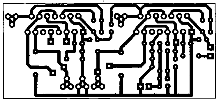
Printed circuit board and installation
The installation is carried out on a compact printed circuit board (Fig. 2). The pattern of the printed tracks is shown as if you were looking at the tracks. If you plan to make the board using a photo method or a “laser iron”, this drawing will need to be made mirrored (this can be done from a scan in any graphics editor).

Rice. 2. Printed circuit board for a bridge power amplifier circuit with a TDA2005 chip.
But, in my opinion, such a simple layout can be drawn manually with a permanent marker. The microcircuit requires a heatsink to operate. I don’t recommend turning it on even temporarily without a radiator. This ULF board can be used for another purpose, not only as a repair module, but also as an automotive ULF.
State Committee of the Russian Federation for Higher Education
Ural State Technical University - UPI
Department of REIS
DIPLOMA THESIS ON THE TOPIC:
BRIDGED AUDITION POWER AMPLIFIER
Ekaterinburg 2006
Introduction
1. Purpose of the work
2. Terms of reference
3. Operating principle of the bridge UMZCH circuit
4. Preparing the boot file
4.1 Drawing up a description of the circuit model
4.2 Selecting design analysis procedures
4.2.1 Options map.
4.2.2 Print bus installation map.
4.2.3 Temperature setting map.
4.2.4 DC sensitivity calculation map.
4.2.5 Calculation of transmission coefficient in small signal mode.
4.2.6 Calculation of the spectral density of internal noise.
4.2.7 Transition analysis.
4.2.8 Fourier harmonic analysis.
4.2.9 Analysis on alternating current.
4.2.10 Printing results.
4.2.11 Monte Carlo method.
4.2.12 Data preparation map for PROBE.
4.3 Compiling a boot file
5. Debugging the circuit model
6. Analysis of the results of machine calculations
6.1 The influence of temperature on the operation of the circuit
6.2 Spectral density of internal noise
6.3 Amplifier transient response
6.4 Fourier harmonic analysis
6.5 Frequency response
6.6 Monte Carlo analysis
6.7 Determining circuit sensitivity
Conclusion
Bibliography
Appendix 1
Appendix 2
Introduction
An audio frequency power amplifier (AMP) is designed to transmit a signal from an excitation source to a load while simultaneously amplifying the signal in terms of power. UMZCH can also be considered as a generator in which the energy of the power source is converted into the energy of an alternating signal under the influence of an input voltage of a certain amplitude. Therefore, UMZCHs are also called generators with external excitation.
UMZCH are generally characterized by the following parameters:
Pout – output power;
K – gain;
Efficiency – efficiency factor;
DF – operating frequency range;
AFC – amplitude-frequency response;
N – level of nonlinear distortion;
Ш – intrinsic noise level.
This work examines the UMZCH bridge, the characteristic features of which are:
maximum use of power supply voltage;
high output power compared to other simple UMZCH;
high circuit stability;
wide range of reproducible frequencies in rated power mode;
relatively low harmonic distortion.
1. Purpose of the work
Coursework provides the student with the following main opportunities:
learn to analyze the technical specifications (TOR) for the design of radio-electronic circuits (RES);
gain the skills to search for scientific and technical literature and work with it, correctly compile and execute technical documentation;
understand the basic concepts and terms related to computer-aided design of electronic distribution systems;
get acquainted with the basic design procedures for analyzing the circuit design stage of electronic equipment;
get acquainted with the modern Pspice application package for circuit design;
learn to set and perform circuit design tasks;
consolidate and deepen knowledge of methods for calculating RES and the elemental base of REA.
2. Terms of reference
Design a bridge UMZCH using data from Radio magazine No. 1/1992
Technical requirements for UMZCH:
Nominal input voltage 0.35 V
Rated (maximum) output power at
load resistance 4 Ohm 16 (20) W
Nominal frequency range 40…20000 Hz
Output voltage slew rate 25 V/µs
Harmonic distortion at rated power at
Schematic electrical diagram of a bridge UMZCH
Fig. 1. Schematic diagram of the bridge UMZCH.
3. Operating principle of the bridge UMZCH circuit
UMZCH consists of two amplifiers. Let's consider one of them based on a power amplifier. Transistor VT1 operates in the voltage amplification stage, and the remaining VT2-VT5 (all with low saturation voltages Us) form a composite emitter power amplification follower operating in AB mode (quiescent current 20...30 mA).
Diodes VD1 and VD2 improve the thermal stability of the quiescent current. Transistor VT3 provides the necessary drive for transistor VT5. In order to maximize the use of the power supply voltage, two positive voltage feedback circuits (POF) are introduced into the amplifier. With a positive half-wave of the amplified signal, circuit R5R6C3 operates, and with a negative half-wave, R8R9C4.
A distinctive feature of such feedback is its introduction into the collector circuit of transistors VT2, VT3, which leads to an increase in the amplitude of the signal at the output of the amplifier to the maximum possible.
In order to reduce nonlinear distortions caused by the asymmetry of the arm-end stage and the action of the PIC, the amplifier is covered by a general negative voltage feedback (NFE) through the circuit R1 - R4C1. The parameters of this circuit are selected in such a way as to, on the one hand, ensure the stability of the amplifier operating mode according to direct current (due to the action of galvanic feedback through resistor R4), and on the other hand, to obtain the required gain of the entire amplifier (R1, R4). The feedback depth for alternating voltage is about 28 dB. Capacitors C2 and C4 provide the necessary stability of the entire amplifier.
Since the described base amplifier is inverting, in order to simplify the circuit, the signal to the second amplifier is supplied from the output of the first through a voltage divider R10R11.
4. Preparing the boot file
4.1 Drawing up a description of the circuit model
At this stage, the input language Pspace, commands for executing design procedures, auxiliary and service tools, and built-in models of RES components were studied.
The initial circuit contains nodes that form the basis for the description of the circuit. Circuit elements are described using the nodes to which they are connected and their nominal values. Moreover, resistors and capacitors are described directly, but for diodes and transistors, their models are required, which are located in electronic libraries.
4.2 Selecting design analysis procedures
4.2.1 Options map
OPTIONS ACCT NOECHO NOPAGE RELTOL =0.0001
ACCT- provides in the output file static information about the simulated circuit and information about the computing resources used - processor time for performing various analysis procedures;
NOECHO prohibits printing the input file in the output file;
NOPAGE prohibits page numbering, printing of the title line and heading for each type of analysis in the output file;
RELTOL – Sets the relative error of voltage and current.
4 .2.2 Print bus installation map
WIDTH OUT=80
The number 80 sets the number of columns in the output file.
4.2.3 Temperature setting map
TEMP 27 –60 80
This card is required to ensure that all analyzes are performed at three different temperatures.
4.2.4 Card for calculating DC sensitivity
SENS V(13,18),
Using this map, small-signal sensitivities of output variables to changes in internal parameters at direct current are calculated.
4.2.5 Calculation of gain in small signal mode
TF V (13,18) VIN ,
where VIN is the input signal generator.
Using this directive, the small signal DC gain, input and output impedance of the amplifier are calculated.
4.2.6 Calculation of the spectral density of internal noise
NOISE V(13,18) VIN
Because resistors and volume resistances of transistors are sources of thermal noise. In addition, semiconductor devices have shot noise and flicker noise. Using the .NOISE map, the spectral density of the internal noise voltage is calculated at each frequency analysis frequency, which is recalculated to the input of the circuit and to its output.
4.2.7 Transition analysis
TRAN/OP 1U 3M
This directive is used to calculate the circuit's response to a given input stimulus. The OP key is required to display detailed information about the operating point.
4.2.8 Fourier harmonic analysis
FOUR V (6) V (13,18)
This card performs Fourier spectral analysis.
FOUR V(6) – harmonic distortion at the circuit input;
Low-frequency power amplifier of the Hi-Fi class, made using a bridge circuit using two TDA7294 integrated circuits. Allows you to get up to 170 watts of output power, perfect for a subwoofer.
Specifications
- Output power at 8 Ohm load and power supply ±25V - 150 W;
- Output power at 16 Ohm load and ±35V power supply - 170 W.
Schematic diagram
The amplifier has output stage protection against short circuit, thermal protection (switching to reduced power in case of overheating that occurs under heavy loads), surge protection, shutdown mode (Standby), input signal on/off mode (Mute), and protection from a “click” when turning on/off. All this has already been implemented in TDA7294 integrated circuits.
Rice. 1. Bridge circuit for connecting two TDA7294 microcircuits - a powerful bridge low-frequency amplifier.
Parts and PCB
Rice. 2. Printed circuit board for the bridge version of the inclusion of TDA7294 microcircuits.

Rice. 3. Location of components for the bridge version of the inclusion of TDA7294 microcircuits.
To power such a power amplifier, you need a power source with a transformer with a power of at least 250-300 watts. In the rectifier circuit, it is advisable to install electrolytic capacitors of 10,000 μF or more on each arm.
Bridge circuit from the datasheet

Rice. 4. Bridge circuit for connecting two TDA7294 microcircuits (from the datasheet).
In bridge mode, the load resistance must be at least 8 ohms, otherwise the microcircuits will burn out from overcurrent!
PCB
Universal printed circuit board for two-channel and bridged power amplifier options.
The bridge circuit for switching on the UMZCH consists of two identical channels, in one of which the signal input is connected to ground, and the feedback input (leg 2) is connected through a 22K resistor to the output of the second channel.
Also, the 10th legs of the microcircuits (Mute) and the 9th legs (Stand-By) need to be connected to a mode control circuit assembled using resistors and capacitors (Figure 6).

Rice. 5. Printed circuit board for a power amplifier based on TDA7294 chips.
The boards have slight deviations (for the better) from the diagram from the datasheet:
- At the inputs of the microcircuits (pin 3), 4 µF capacitors are installed, not 0.56 µF;
- A 470 µF capacitor is connected between the 680 Ohm resistor (which goes to pin 2) and ground;
- The capacitors between legs 6 and 14 are 470 µF, not 22 µF;
- For power supply, instead of 0.22 µF capacitors, it is proposed to install 680 nF (0.68 µF);
In a bridge connection, pins 10 and 9 are connected together respectively and connected to the mode control circuit.

Rice. 6. A simple control circuit for Standby-Mute modes for TDA7294 chips.
To turn on the microcircuits (take them out of quiet and energy-saving modes), the “VM” and “VSTBY” contacts just need to be connected to the positive +Vs power supply pin.
This printed circuit board is universal; it can be used for both dual-channel and bridge modes of operation of the amplifier on TDA7294 chips. The ground wiring (GND) is very well done here, which will improve the reliability and noise immunity of the UMZCH.
Literature:
- Datasheet for the TDA7294 chip - Download (7-Zip archive, 1.2MB).
- FAQ for TDA7294 - cxem.net/sound/amps/amp129.php
Assembling a car subwoofer with your own hands is quite an honorable task, but there are often difficulties with assembling the power amplifier that should power the subwoofer head. For fairly powerful heads, the standard 12 Volt network is not enough, and you need to increase the voltage with a voltage converter.
It’s not possible to achieve high power without using a converter, but what to do if you don’t have the proper experience in building a converter, but you really want to build an amplifier for a subwoofer?
According to the laws of physics, it is impossible to obtain more than 18 watts of power from a 12 Volt network into a 4 Ohm load - we are talking about pure, sinusoidal output power, but as always there are exceptions. There is a variety of amplifiers operating in class H, which allow you to get an output power of 50-70 watts from a 12 Volt network, but such microcircuit amplifiers (for example, TDA1562) are very expensive, therefore, you need to look for another solution.
Today we will consider one of the cheapest options for UMZCH for a subwoofer. The well-known TDA2003 microcircuit is at least the cheapest UMZCH microcircuit. It is powered by 12 Volts and can provide a maximum power of up to 10-12 watts into a 2 ohm load.
The main advantage of the microcircuit itself is that it can work with low-impedance dynamic heads with coil resistance up to 2 ohms. The microcircuit is monophonic in nature (single-channel), therefore there must be a bridge circuit that will increase the output power of the amplifier.
The bridge version works great with standard 4 Ohm heads for a long time, the output power is around 20 Watts, peak surges during deep low frequencies are up to 30 Watts, but of course this is not pure power. But it is quite possible to power a medium-power subwoofer using this option.
The second feature of this option is that the microcircuit costs a penny (half a dollar apiece), the element base contains only a few components, with a total cost of no more than a dollar, but if you have old boards, you can unsolder all the necessary components from them.
The microcircuit operates in class AB, therefore it is impossible to avoid overheating, so the microcircuits must be installed on a common heat sink, and there is no need to use additional insulating gaskets, since the mass of the microcircuits is the same.
Well, yes - we don’t have the part number and number of channels right now - what can you do about it.
Now we will talk about 4 channel amplifiers. For the most part, they are used for automotive use, but, in principle, nothing prevents them from being used at home - their characteristics are quite decent, especially the latest generation.
Let's start with TDA7560, production SGS-Thomson. As usual, this is a class AB bridge amplifier with all kinds of protections and functions Mute And StanBy, and just as you will see in the diagram - the almost complete absence of hanging elements.
Well, this microcircuit also works great at a load of 2 Ohms.
Connection diagram:
That is, in fact, you take a microcircuit, attach inputs and outputs to it, and everything works. Fairy tale.
This creation is produced in a case Flexiwatt25- again with half holes on the sides.
Our next patient is a microcircuit TDA8571J from Philips Semiconductors. With this amplifier, the comrades decided to show off and made it a bridge amplifier, like everyone else, but at the same time - class B. And for the rest, as usual - a full set of output protection and temperature protection. Moreover, like the previous one being prepared, practically no attachments are required.
The main characteristics are as follows:
Connection diagram:

And the amp is bare.
Well, if you just go to the entrance Mute hang. All this is happily in the building SOT411-1, again with half holes on the sides.
That's all - the last one is enough.
This time the last one will be the amplifier TDA8591 still the same Philips Semiconductors. In terms of its characteristics, it is similar to the previous speaker, however, it can work with a 2-ohm load and is somewhat more powerful. Plus, it has a pretty clever DC output voltage detection circuit.
The main characteristics are as follows:
Connection diagram:

Well, in general, nothing particularly terrible, you just need to take into account that for the amplifier to work, the button S1 needs to be closed. Otherwise, he will remain partisan silent.
As for the DC output voltage detection circuit, if you don’t need it, you can throw out almost half of the passive components from the circuit. Let's list these heroes by name: R1-R6, C14. And we connect pin 26 of the microcircuit to the common wire.
Well, that's all for now. Of course, we don’t end the Bridjump theme here - in fact, we’ve only just begun.